
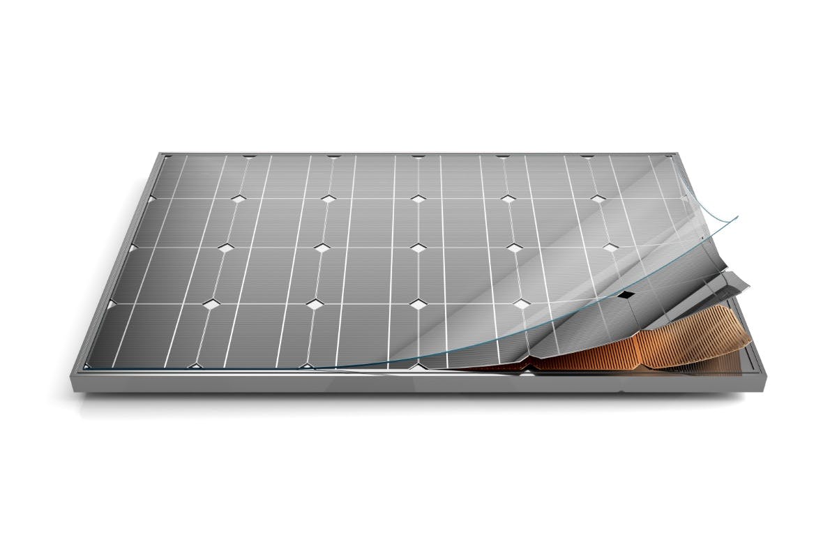
There are several stages involved in the construction of solar cells. To let light through the material, the p-type area is thin. The junction is formed from thin n-material. The n material's bottom is covered with a metal plating. They are joined together in a series, and are surrounded with a glass window.
Pn-junction solar cell
A Pn junction solar cell has three layers. The top junction is made of silicon, while the absorber layer and the back junction are made of P material. The top junction can be made of silicon and the absorber layer is made of thin layers of P material. This allows incident light photos to reach the junction. These photons allow electrons to escape from their parent molecules, creating free electrons on both sides. A current flows when there are light-induced changes of the electrical charge within the cell's layers. It is directly proportional in magnitude to the amount of illumination. Likewise, the open circuit voltage is proportional to the amount of illumination the cell receives.
The p/n junction is made up two layers. It is arranged in such a way that electrons of the n layer move towards and fill the holes in the nearby p/type layer. The pn junction is a small, battery-cell-like device that can produce photovoltage. This produces a tiny current every time a small load passes through the pn junction.
Single-junction silicon solar cell
A single-junction solar cell uses two layers. The lower one contains a lower amount of electrons while the upper one has a higher number. The lower layer of silicon is known as positive-type silicon and the upper is known as negative-type. This junction allows for current to flow between the two layers.

Since decades, single-junction cells have been extensively studied. For 1-sun conditions they have a practical efficiency rate of 26%. They can be combined with cells with large bandgap energy, which convert short wavelength photons to generate voltage. The growth of dual-junction cells can also help reduce thermalization losses, and produce a high external-radiative efficiency.
Solar cells can be used in series-parallel combinations
A series-parallel combination can improve the solar cells' voltage and current generation. It is often used to build solar panels. It is used to build solar panels. A series-parallel arrangement uses single solar cells that are connected together to create solar modules.
The area of a photovoltaic cell directly influences the amount of electric current it produces. The bigger the cell, so the electricity produced will be higher. These quantities are measured by Isc (short-circuit current) and Jsc (current density). The current density and voltage are usually higher if the short circuit current is higher.
Reflective layer
An reflective layer can be added to a solar cell to increase its energy production. It is a thin layer of material that acts as a barrier between the semiconductor and air. The layer is normally made from a material that has the same refractive index as the semiconductor. The film reflects light in two directions: at the air-semiconductor interface and at the substrate-solar cell interface. A high-quality AR layer will reduce the number of reflection points.
The reflective layer (or last layer) is the last layer in a solar cells. Its purpose is to decrease light loss in the system. There are many options available depending on the application and the cost.
Base layer
The base layer of any solar cell is made from silicon. It serves as an antireflection coating, which reduces light loss from reflection and promotes light transmission to the energy conversion layers below. This layer is usually made from silicon oxide, tantalum or titanium and is formed by spin-coating or vacuum evaporation.
The base layer of a solar cell absorbs light at an extremely high efficiency. It is composed of two layers, the silicon n-type layer and the silicon p-type layer. The n type silicon layer is composed of fewer positively charged holes (called “vacancies”), while the p type silicon contains many negatively charged electrons. The lack of any valence electrons causes the vacancies. This causes electrons on one side to move to the opposing side of the junction. This phenomenon is known as the depletion area.